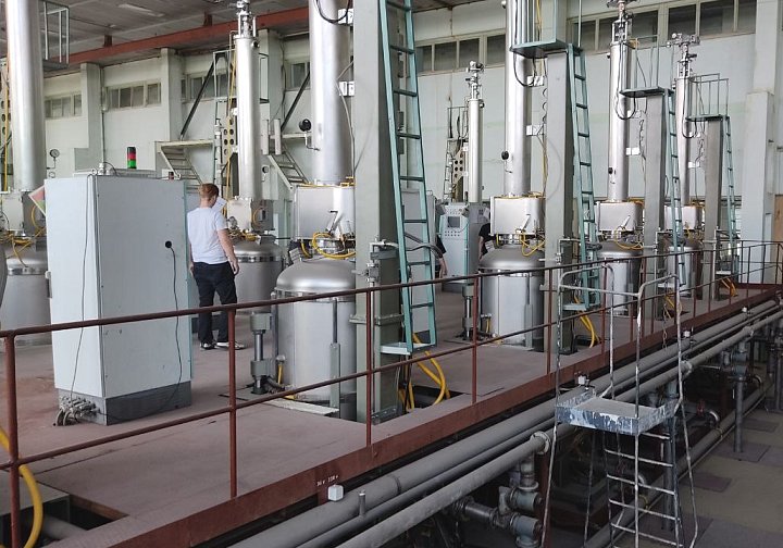
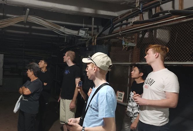
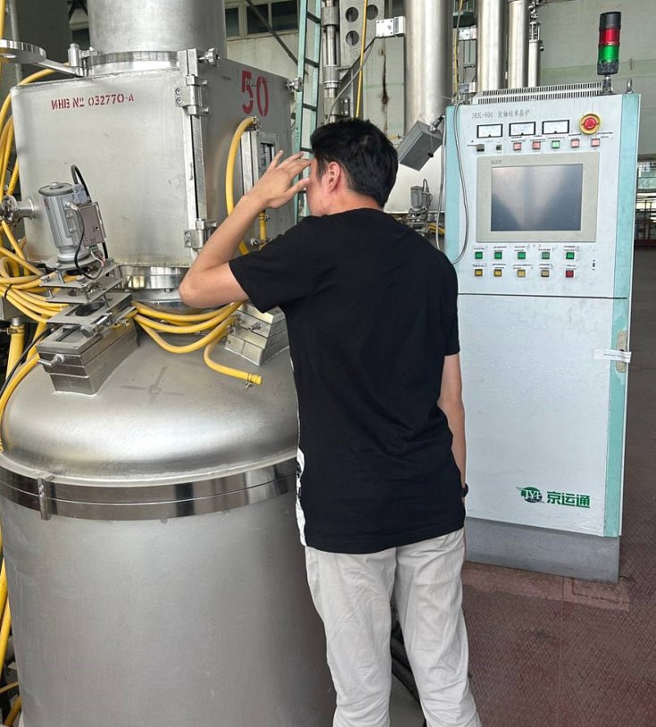
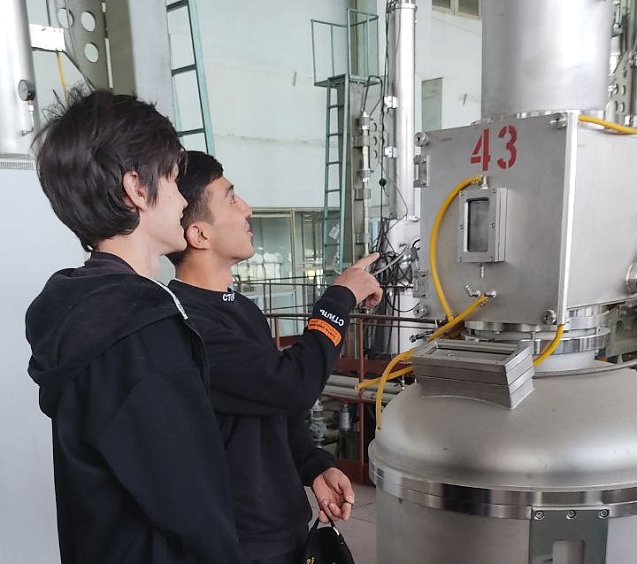

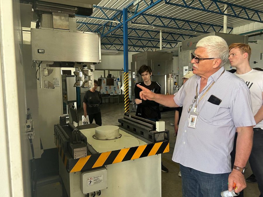
Practice is one of the mandatory parts of the educational process, allowing students to get acquainted with the real technological process in enterprises and consolidate theoretical knowledge. This year, students of the Department of Physics and Microelectronics got acquainted with the work of OJSC «Kyrgyz Chemical and Metallurgical Plant» in Orlovka.
This company grows single-crystal silicon and also produces wafers for photovoltaic modules that convert sunlight into electrical energy. The company is the only enterprise in the CIS producing single-crystal ingots and plates using HJT technology for the solar energy market.
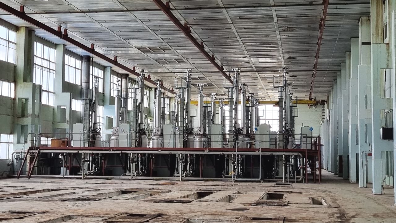
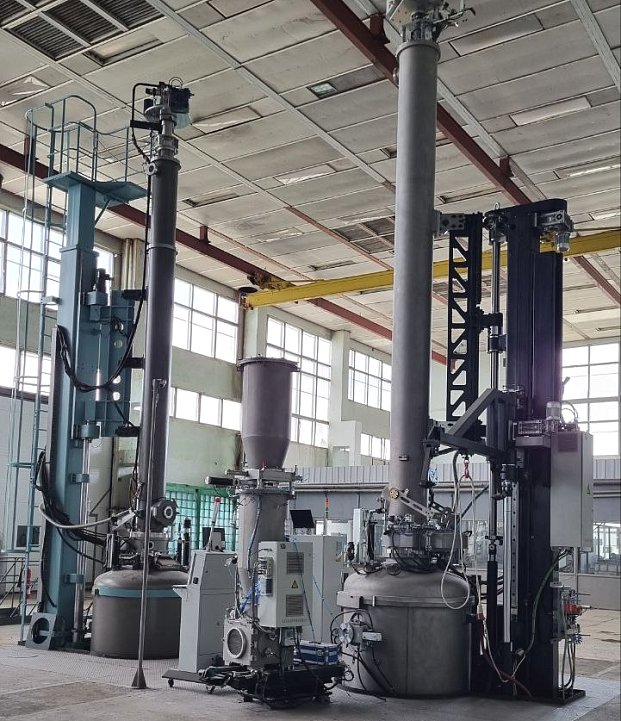
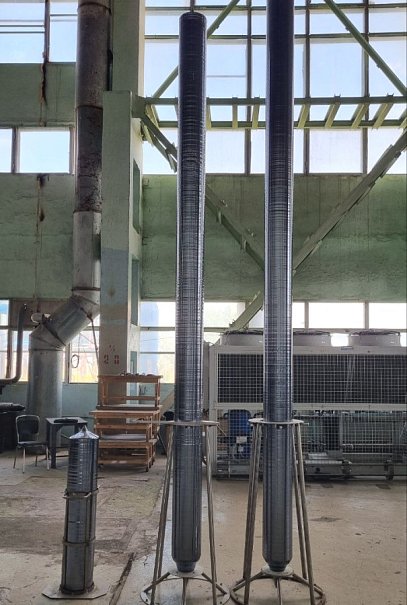
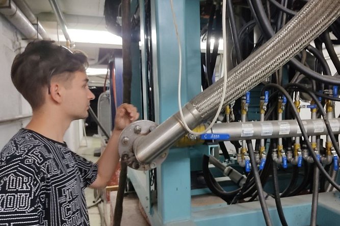
During the excursion, the director of the enterprise described the technology and showed the furnaces used for growing silicon single crystals. Students also saw production lines where the resulting ingots, several meters long, are cut, cut into plates, etched, ground and packaged.
The next point of on-site internship for students was the high-mountain observatory of physics of atmospheric processes KRSU and the scientific station of the Russian Academy of Sciences, located in the village of Teploklyuchenka, Issyk-Kul region.
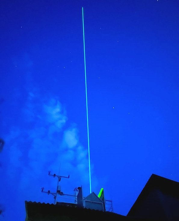
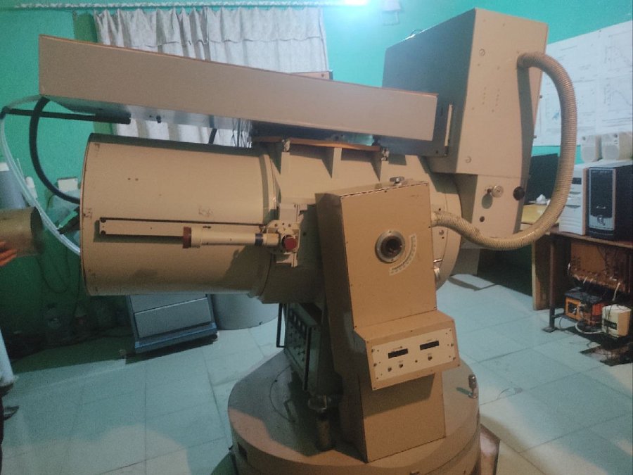
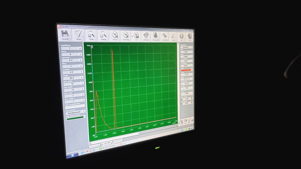
The long, many-hour journey to the high-mountain observatory allowed the staff not only to give students a lecture on the method of lidar sensing of the atmosphere, the study of the optical and microphysical characteristics of the tropospheric aerosol, and the unique equipment of the lidar complex, but also to show how night measurements are carried out. The students were especially struck by a green laser beam rising several kilometers into the sky.
The next day, during the journey home, the students stopped briefly at the boarding house KRSU «Zhashtyk» so that the sea air and highlands would give them a boost of energy to successfully complete their internship and school year.